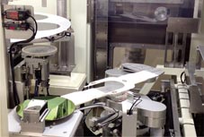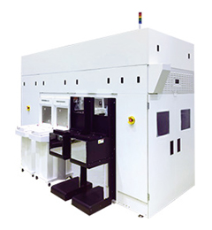

Automated Wafer Transportation System
for LED/Power Semiconductor
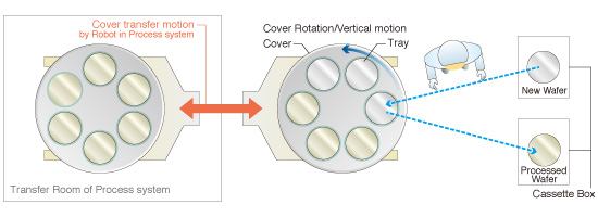
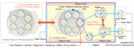
New Transfer Unit
Applicable for increasing size of LED/Power Semiconductor Wafer
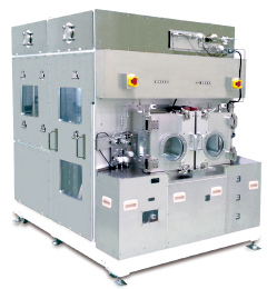
 300/200mm Wafer mapping function (No Change Required)
Power saving technology by Auto set and transfer Wafer between Cassette and Process system
High yield due to handling in clean N2 atmosphere (by N2 Circulation)
(decrease particle, moisture and O2)
High productivity due to capable of handling hot Wafer after process